- 您现在的位置:买卖IC网 > Sheet目录2000 > IDTCV136PAG (IDT, Integrated Device Technology Inc)IC FLEXPC CLK ATI RS400 56-TSSOP
COMMERCIALTEMPERATURERANGE
IDTCV136
PROGRAMMABLEFLEXPC CLOCKFORATIRS400
11
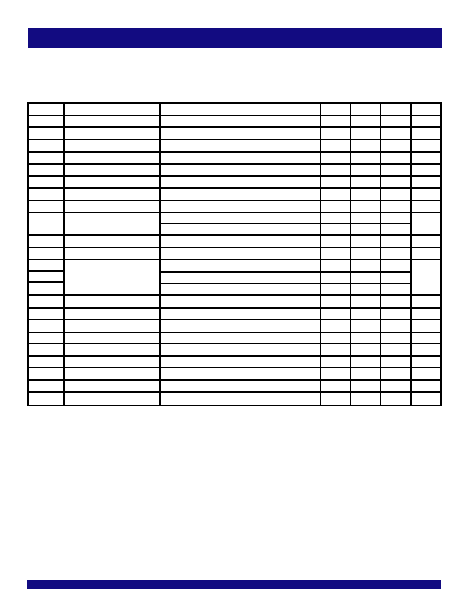
Symbol
Parameter
Test Conditions
Min.
Typ.
Max.
Unit
VIH
Input HIGH Voltage
3.3V ± 5%
2
—
VDD + 0.3
V
VIL
Input LOW Voltage
3.3V ± 5%
VSS - 0.3
—
0.8
V
VIH_FS
3.3V Input HIGH Voltage
VDD
0.7
—
VDD + 0.3
V
VIL_FS
3.3V Input LOW Voltage
VSS - 0.3
—
0.35
V
IIH
Input HIGH Current
VIN = VDD
–5
—
5
A
IIL1
Input LOW Current
VIN = 0V, inputs with no pull-up resistors
–5
—
A
IIL2
Input LOW Current
VIN = 0V, inputs with pull-up resistors
–200
—
A
IDD3.3OP
Operating Supply Current
Full active, CL = full load
—
400
mA
IDD3.3PD
Powerdown Current
All differential pairs driven
—
70
mA
All differential pairs tri-stated
—
12
FI
Input Frequency(1)
VDD = 3.3V
—
14.31818
—
MHz
LPIN
Pin Inductance(2)
——
7
nH
CIN
Logic inputs
—
5
COUT
Input Capacitance(2)
Output pin capacitance
—
6
pF
CINX
X1 and X2 pins
—
5
Modulation Frequency(2)
Triangular modulation
30
—
33
KHz
TSU_PD#
Stop response of all clocks after PD# assertion
—
100
ns
TSTAB
Clock Stabilization(2,3)
From VDD power-up or de-assertion of PD# to first clock
—
1.8
ms
TRISE_PD#(2)
Rise time of PD#
—
5
ns
TFALL_PD#(2)
Fall time of PD#
—
5
ns
TSU_CPU(2)
CPU output disable after CPU_Stop# assertion
—
60
ns
TDRIVE_CPU_Stop#(2)
CPU output enable after CPU_Stop# de-assertion
—
60
ns
TSU_SRC(2)
SRC output disable after CLKREQ# assertion
—
60
ns
TDRIVE_SRC(2)
SRC output enable after CLKREQ# de-assertion
—
60
ns
ELECTRICAL CHARACTERISTICS - INPUT / SUPPLY / COMMON OUTPUT
PARAMETERS
Following Conditions Apply Unless Otherwise Specified:
Operating Condition: TA = 0°C to +70°C, Supply Voltage: VDD = 3.3V ± 5%
NOTES:
1.
Input frequency should be measured at the REF output pin and tuned to ideal 14.31818MHz to meet ppm frequency accuracy on PLL outputs.
2.
This parameter is guaranteed by design, but not 100% production tested.
3.
See TIMING DIAGRAMS for timing requirements.
发布紧急采购,3分钟左右您将得到回复。
相关PDF资料
IDTCV137PAG
IC FLEXPC CLK AMD K8 56-TSSOP
IDTCV142PAG
IC FLEXPC CLK PROGR P4 56-TSSOP
IDTCV146PVG
IC FLEXPC CLK PROGR P4 56-SSOP
IDTCV149PAG
IC FLEXPC CLK PROGR K8 56-TSSOP
IDTNW6005ASG
IC CALLER ID DECODER 20SOIC
IDTNW6006AS
IC CALLER ID DECODER 20-SOIC
IDTSSTE32882HLBBKG
IC REGISTERING CLK DRIVER 176BGA
IDTSSTE32882KA1AKG
IC REGISTERING CLK DRIVER 176BGA
相关代理商/技术参数
IDTCV136PAG8
功能描述:IC FLEXPC CLK ATI RS400 56-TSSOP RoHS:是 类别:集成电路 (IC) >> 时钟/计时 - 专用 系列:FlexPC™, PCI Express® (PCIe) 标准包装:28 系列:- 类型:时钟/频率发生器 PLL:是 主要目的:Intel CPU 服务器 输入:时钟 输出:LVCMOS 电路数:1 比率 - 输入:输出:3:22 差分 - 输入:输出:无/是 频率 - 最大:400MHz 电源电压:3.135 V ~ 3.465 V 工作温度:0°C ~ 85°C 安装类型:表面贴装 封装/外壳:64-TFSOP (0.240",6.10mm 宽) 供应商设备封装:64-TSSOP 包装:管件
IDTCV137PAG
功能描述:IC FLEXPC CLK AMD K8 56-TSSOP RoHS:是 类别:集成电路 (IC) >> 时钟/计时 - 专用 系列:FlexPC™, PCI Express® (PCIe) 标准包装:1,500 系列:- 类型:时钟缓冲器/驱动器 PLL:是 主要目的:- 输入:- 输出:- 电路数:- 比率 - 输入:输出:- 差分 - 输入:输出:- 频率 - 最大:- 电源电压:3.3V 工作温度:0°C ~ 70°C 安装类型:表面贴装 封装/外壳:28-SSOP(0.209",5.30mm 宽) 供应商设备封装:28-SSOP 包装:带卷 (TR) 其它名称:93786AFT
IDTCV137PAG8
功能描述:IC FLEXPC CLK AMD K8 56-TSSOP RoHS:是 类别:集成电路 (IC) >> 时钟/计时 - 专用 系列:FlexPC™, PCI Express® (PCIe) 标准包装:28 系列:- 类型:时钟/频率发生器 PLL:是 主要目的:Intel CPU 服务器 输入:时钟 输出:LVCMOS 电路数:1 比率 - 输入:输出:3:22 差分 - 输入:输出:无/是 频率 - 最大:400MHz 电源电压:3.135 V ~ 3.465 V 工作温度:0°C ~ 85°C 安装类型:表面贴装 封装/外壳:64-TFSOP (0.240",6.10mm 宽) 供应商设备封装:64-TSSOP 包装:管件
IDTCV140
制造商:IDT 制造商全称:Integrated Device Technology 功能描述:PROGRAMMABLE FLEXPC CLOCK FOR P4 PROCESSOR
IDTCV141PAG
功能描述:IC CLK BUFFER 1-8 DIFF 48-TSSOP RoHS:是 类别:集成电路 (IC) >> 时钟/计时 - 专用 系列:- 标准包装:1 系列:- 类型:时钟/频率发生器,多路复用器 PLL:是 主要目的:存储器,RDRAM 输入:晶体 输出:LVCMOS 电路数:1 比率 - 输入:输出:1:2 差分 - 输入:输出:无/是 频率 - 最大:400MHz 电源电压:3 V ~ 3.6 V 工作温度:0°C ~ 85°C 安装类型:表面贴装 封装/外壳:16-TSSOP(0.173",4.40mm 宽) 供应商设备封装:16-TSSOP 包装:Digi-Reel® 其它名称:296-6719-6
IDTCV141PAG8
功能描述:IC CLK BUFFER 1-8 DIFF 48-TSSOP RoHS:是 类别:集成电路 (IC) >> 时钟/计时 - 专用 系列:- 标准包装:28 系列:- 类型:时钟/频率发生器 PLL:是 主要目的:Intel CPU 服务器 输入:时钟 输出:LVCMOS 电路数:1 比率 - 输入:输出:3:22 差分 - 输入:输出:无/是 频率 - 最大:400MHz 电源电压:3.135 V ~ 3.465 V 工作温度:0°C ~ 85°C 安装类型:表面贴装 封装/外壳:64-TFSOP (0.240",6.10mm 宽) 供应商设备封装:64-TSSOP 包装:管件
IDTCV141PVG
功能描述:IC CLK BUFFER 1-8 DIFF 48-SSOP RoHS:是 类别:集成电路 (IC) >> 时钟/计时 - 专用 系列:- 标准包装:28 系列:- 类型:时钟/频率发生器 PLL:是 主要目的:Intel CPU 服务器 输入:时钟 输出:LVCMOS 电路数:1 比率 - 输入:输出:3:22 差分 - 输入:输出:无/是 频率 - 最大:400MHz 电源电压:3.135 V ~ 3.465 V 工作温度:0°C ~ 85°C 安装类型:表面贴装 封装/外壳:64-TFSOP (0.240",6.10mm 宽) 供应商设备封装:64-TSSOP 包装:管件
IDTCV141PVG8
功能描述:IC CLK BUFFER 1-8 DIFF 48-SSOP RoHS:是 类别:集成电路 (IC) >> 时钟/计时 - 专用 系列:- 标准包装:28 系列:- 类型:时钟/频率发生器 PLL:是 主要目的:Intel CPU 服务器 输入:时钟 输出:LVCMOS 电路数:1 比率 - 输入:输出:3:22 差分 - 输入:输出:无/是 频率 - 最大:400MHz 电源电压:3.135 V ~ 3.465 V 工作温度:0°C ~ 85°C 安装类型:表面贴装 封装/外壳:64-TFSOP (0.240",6.10mm 宽) 供应商设备封装:64-TSSOP 包装:管件